(Electronic Components) 5V927PGGI8
Product Attributes
| TYPE | DESCRIPTION |
| Category | Integrated Circuits (ICs) |
| Mfr | Renesas Electronics America Inc |
| Series | - |
| Package | Tape & Reel (TR) |
| Product Status | Obsolete |
| Type | Clock Generator |
| PLL | Yes with Bypass |
| Input | LVTTL, Crystal |
| Output | LVTTL |
| Number of Circuits | 1 |
| Ratio – Input:Output | 2:4 |
| Differential – Input:Output | No/No |
| Frequency – Max | 160MHz |
| Divider/Multiplier | Yes/No |
| Voltage – Supply | 3V ~ 3.6V |
| Operating Temperature | -40°C ~ 85°C |
| Mounting Type | Surface Mount |
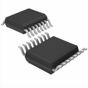
| Package / Case | 16-TSSOP (0.173″, 4.40mm Width) |
| Supplier Device Package | 16-TSSOP |
| Base Product Number | IDT5V927 |
Documents & Media
| RESOURCE TYPE | LINK |
| Datasheets | IDT5V927 |
| PCN Obsolescence/ EOL | Revision 23/Dec/2013 |
| HTML Datasheet | IDT5V927 |
Environmental & Export Classifications
| ATTRIBUTE | DESCRIPTION |
| Moisture Sensitivity Level (MSL) | 1 (Unlimited) |
| REACH Status | REACH Unaffected |
| ECCN | EAR99 |
| HTSUS | 8542.39.0001 |
Additional Resources
| ATTRIBUTE | DESCRIPTION |
| Other Names | 5V927PGGI8 |
| Standard Package | 4,000 |
Product Details
24-BIT DIGITAL SIGNAL PROCESSOR
The Motorola DSP56307, a member of the DSP56300 family of programmable digital signal processors (DSPs), supports wireless infrastructure applications with general filtering operations. The on-chip enhanced filter coprocessor (EFCOP) processes filter algorithms in parallel with core operation, thus increasing overall DSP performance and efficiency. Like the other family members, the DSP56307 uses a high-performance, single-clock-cycle-per-instruction engine (code-compatible with Motorolas popular DSP56000 core family), a barrel shifter, 24-bit addressing, an instruction cache, and a direct memory access controller, as in Figure 1. The DSP56307 offers performance at 100 million instructions (MIPS) per second using an internal 100 MHz clock with 2.5 volt core and independent 3.3 volt input/output power.
Overview
Using the second generation ASMBL (Advanced Silicon Modular Block) column-based architecture, the XC5VLX330T-3FFG1738I contains five distinct platforms (sub-families), the most choice offered by any FPGA family. Each platform contains a different ratio of features to address the needs of a wide variety of advanced logic designs. In addition to the most advanced, high-performance logic fabric, XC5VLX330T-3FFG1738I FPGAs contain many hard-IP system level blocks, including powerful 36-Kbit block RAM/FIFOs, second generation 25 x 18 DSP slices, Select IO technology with built-in digitally-controlled impedance, Chip Sync source-synchronous interface blocks, system monitor functionality,
FEATURES
High-Performance DSP56300 Core
● 100 million instructions per second (MIPS) with a 100 MHz clock at 2.5 V core and 3.3 V I/O
● Object code compatible with the DSP56000 core
● Highly parallel instruction set
● Data arithmetic logic unit (ALU)
- Fully pipelined 24 x 24-bit parallel multiplier-accumulator
- 56-bit parallel barrel shifter (fast shift and normalization; bit stream generation and parsing)
- Conditional ALU instructions
- 24-bit or 16-bit arithmetic support under software control
● Program control unit (PCU)
- Position independent code (PIC) support
- Addressing modes optimized for DSP applications (including immediate offsets)
- On-chip instruction cache controller
- On-chip memory-expandable hardware stack
- Nested hardware DO loops
- Fast auto-return interrupts
● Direct memory access (DMA)
- Six DMA channels supporting internal and external accesses
- One-, two-, and three- dimensional transfers (including circular buffering)
- End-of-block-transfer interrupts
- Triggering from interrupt lines and all peripherals
● Phase-locked loop (PLL)
- Allows change of low power divide factor (DF) without loss of lock
- Output clock with skew elimination
● Hardware debugging support
- On-Chip Emulation (On CE) module
- Joint test action group (JTAG) test access port (TAP)
- Address trace mode reflects internal Program RAM accesses at the external port


