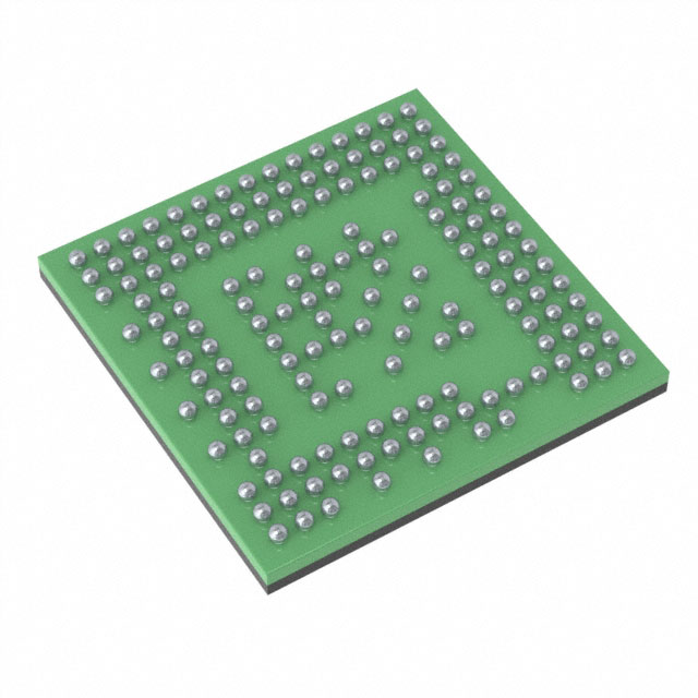
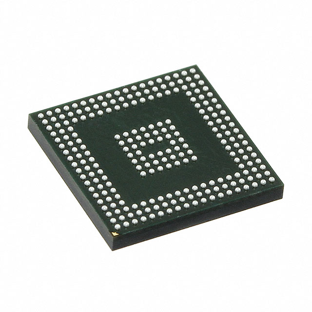
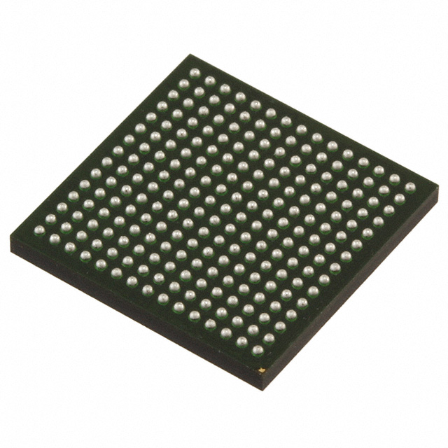
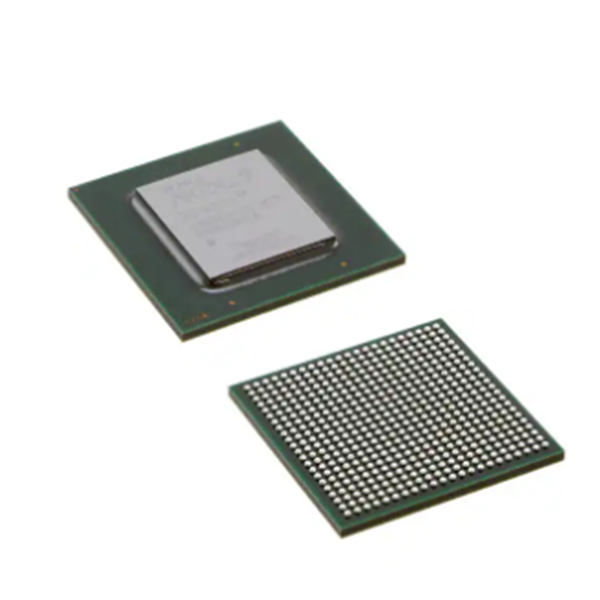
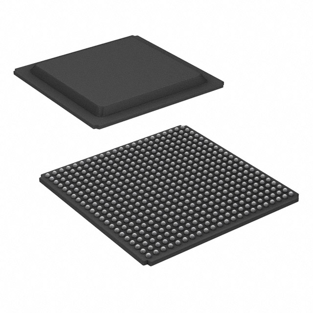
New And Original Electronic Components FCCSP-161 AWR1642ABISABLRQ1 AWR1642ABISABLRQ1
Product Attributes
| TYPE | DESCRIPTION |
| Category | RF/IF and RFID |
| Mfr | Texas Instruments |
| Series | Automotive, AEC-Q100, mmWave, Functional Safety (FuSa) |
| Package | Tape & Reel (TR)
Cut Tape (CT) Digi-Reel® |
| SPQ | 1000T&R |
| Product Status | Active |
| Type | TxRx + MCU |
| RF Family/Standard | RADAR |
| Frequency | 76GHz ~ 81GHz |
| Power - Output | 12.5dBm |
| Serial Interfaces | I²C, JTAG, SPI, UART |
| Voltage - Supply | 1.71V ~ 1.89V, 3.15V ~ 3.45V |
| Operating Temperature | -40°C ~ 125°C (TJ) |
| Mounting Type | Surface Mount |
| Package / Case | 161-TFBGA, FCCSP |
| Supplier Device Package | 161-FC/CSP (10.4x10.4) |
| Base Product Number | AWR1642 |
1.Main uses of silicon products
In the semiconductor industry, silicon materials are mostly used in the manufacture of diodes/transistors, integrated circuits, rectifiers, thyristors, etc. Specifically, diodes/transistors made of silicon materials are mostly used in communications, radar, broadcasting, television, automatic control, etc.; integrated circuits are mostly used in various computers, communications, broadcasting, automatic control, electronic stopwatches, instruments, and meters, etc.; rectifiers are mostly used in rectification; thyristors are mostly used in Rectifiers are mostly used for rectification, DC transmission, and distribution, electrical locomotives, equipment self-control, high-frequency oscillators, etc.; ray detectors are mostly used for atomic energy analysis, light quantum detection; solar cells are mostly used in the field of solar power generation.
2.Is there a future chip material that could replace silicon?
Silicon is the most widely used semiconductor material today, but the emergence of graphene, known as the "king of new materials", has led many experts to predict that graphene could be an excellent alternative to silicon, but it will largely depend on its industrial development.
Why is graphene favored? Apart from its own semiconductor properties, which are not inferior to those of silicon, it also has many advantages that silicon does not possess. As the processing limit for silicon is considered to be 10nm line width, in other words, the less the process is than 10nm, the more unstable the silicon product will be and the more demanding the process will be. To achieve higher levels of integration and performance, new semiconductor materials must be processed, and graphene happens to be a good choice. Scientists have observed the quantum Hall effect in graphene at room temperature, and the material does not backscatter when it encounters impurities, suggesting that it has strong electrical conductivity. In addition, graphene appears almost transparent, and its optical properties are not only excellent but also change with the thickness of the graphene. This property is therefore judged to be well suited to applications in optoelectronics.
Perhaps the reason for the bullishness of graphene also depends on its other identity: carbon nanomaterials. Carbon nanotubes are seamless, hollow tubes made from sheets of graphene rolled into a body with extremely good electrical conductivity and very thin walls. Theoretically, a carbon nanotube chip is smaller than a silicon chip at the same level of integration; in addition, carbon nanotubes themselves produce very little heat, which, combined with their good thermal conductivity, can reduce energy consumption; and in terms of the cost of obtaining the element carbon, it is not difficult to obtain carbon materials, given its wide distribution and equally large content in the earth.
Of course, graphene has now been used in screens, batteries, and wearable devices, and scientists have made considerable progress in this area of research, but overall, if graphene is to truly replace silicon and become the mainstream material for chips, more effort will be needed in the manufacturing process and the technology of the supporting devices.


