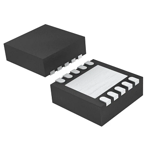
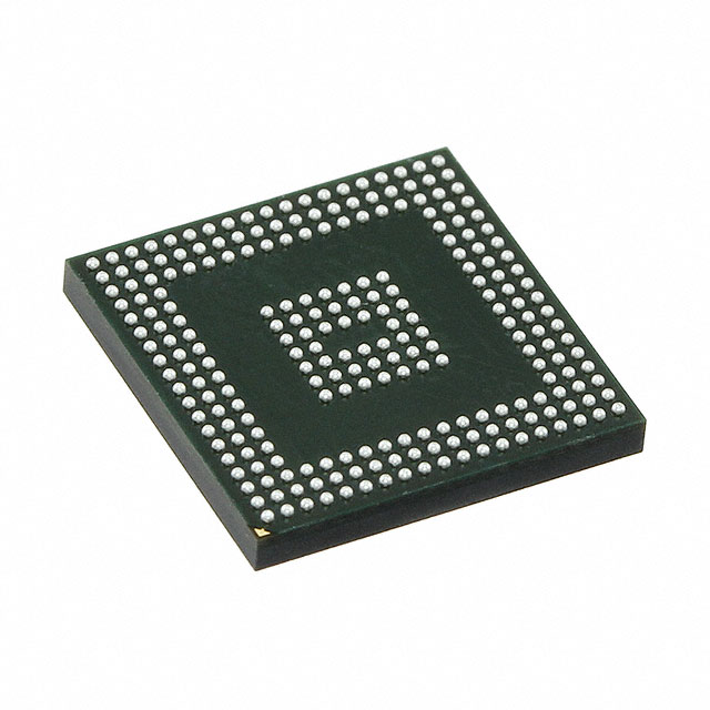
One Stop Service SON8 TPS7A8101QDRBRQ1 With Original And New IC Electronics Chips
Product Attributes
| TYPE | DESCRIPTION |
| Category | Integrated Circuits (ICs) |
| Mfr | Texas Instruments |
| Series | Automotive, AEC-Q100 |
| Package | Tape & Reel (TR)
Cut Tape (CT) Digi-Reel® |
| SPQ | 3000 T&R |
| Product Status | Active |
| Output Configuration | Positive |
| Output Type | Adjustable |
| Number of Regulators | 1 |
| Voltage - Input (Max) | 6.5V |
| Voltage - Output (Min/Fixed) | 0.8V |
| Voltage - Output (Max) | 6V |
| Voltage Dropout (Max) | 0.5V @ 1A |
| Current - Output | 1A |
| Current - Quiescent (Iq) | 100 µA |
| Current - Supply (Max) | 350 µA |
| PSRR | 48dB ~ 38dB (100Hz ~ 1MHz) |
| Control Features | Enable |
| Protection Features | Over Current, Over Temperature, Reverse Polarity, Under Voltage Lockout (UVLO) |
| Operating Temperature | -40°C ~ 125°C (TJ) |
| Mounting Type | Surface Mount |
| Package / Case | 8-VDFN Exposed Pad |
| Supplier Device Package | 8-SON (3x3) |
| Base Product Number | TPS7A8101 |
An LDO, or low dropout regulator, is a low dropout linear regulator that uses a transistor or field effect tube (FET) operating in its saturation region to subtract excess voltage from the applied input voltage to produce a regulated output voltage.
The four main elements are Dropout, Noise, Power Supply Rejection Ratio (PSRR), and Quiescent Current Iq.
The main components: starting circuit, constant current source bias unit, enabling circuit, adjusting element, reference source, error amplifier, feedback resistor network and protection circuit, etc.
Operating Principle
The LDO basic circuit consists of series regulator VT, sampling resistors R1 and R2, and comparison amplifier A
The system is powered up, if the enable pin is at a high level, the circuit starts, the constant current source circuit provides bias to the whole circuit, the reference source voltage is quickly established, and the unregulated input voltage is used as the voltage of the power supply, the reference voltage is used as the negative phase input voltage of the error amplifier, the resistor feedback network divides the output voltage and obtains the feedback voltage, this feedback voltage is input to the same direction terminal of the error comparator, and the negative This feedback voltage is input to the isotropic side of the error comparator and compared with the negative reference voltage. The difference between the two voltages is amplified by the error amplifier to directly control the gate of the power adjusting element, and the output of the LDO is controlled by changing the conduction state of the adjusting tube, i.e. Vout = (R1 + R2)/R2 × Vref
The actual low dropout linear regulator also has other functions such as load short circuit protection, overvoltage shutdown, thermal shutdown, reverse connection protection, etc.
Advantages, disadvantages, and current status
Low Dropout Voltage (LDO) linear regulators are low cost, low noise, low quiescent current, few external components, usually only one or two bypass capacitors, and have very low own noise and a high Power Supply Rejection Ratio (PSRR). The LDO is a miniature System on Chip (SoC) with very low self-consumption. It can be used for current main channel control and has integrated hardware circuits such as MOSFETs with very low in-line on-resistance, Schottky diodes, sampling resistors, and voltage dividers, as well as over-current protection, over-temperature protection, precision reference sources, differential amplifiers, delayers, etc. The PG is a new generation of LDO with a self-test for each output state and delayed safe power supply, which can also be called Power Good, i.e. "power good or power stable". Many LDOs require only one capacitor at the input and one at the output for stable operation.
New LDOs can achieve the following specifications: output noise of 30µV, PSRR of 60dB, quiescent current of 6µA, and a voltage drop of only 100mV. The main reason for this improved performance of LDO linear regulators is that the regulator used is a P-channel MOSFET, which is voltage-driven and requires no current, reducing the current consumed by the device itself and the voltage drop across it. drop is roughly equal to the product of the output current and the on-resistance. The voltage drop across the MOSFET is very low due to its low on-resistance. Common linear regulators use PNP transistors. In circuits with PNP transistors, the voltage drop between input and output must not be too low to prevent the PNP transistor from going into saturation and reducing the output capability.


.png)
-300x300.png)

