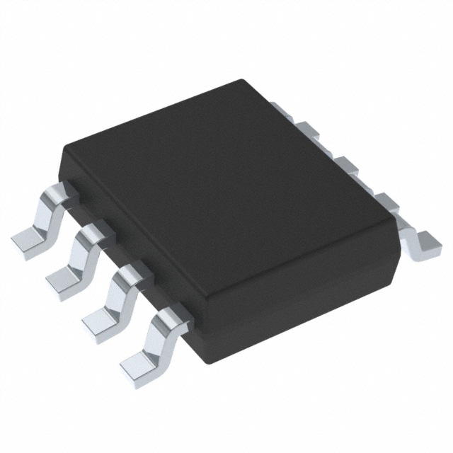
one-stop shop for electronic components TLV1117LV33DCYR SOT223 controller chip ic integrated circuit
A precision bandgap and error amplifier provides 1.5% accuracy. A very high power-supply rejection ratio (PSRR) enables use of the device for postegulation after a switching regulator. Other valuablefeatures include low output noise and low-dropou tvoltage.
The device is internally compensated to be stablewith 0-Ω equivalent series resistance (ESR) capacitors. These key advantages enable the use of cost-effective, small-size ceramic capacitors. Cost-effective capacitors that have higher bias voltagesand temperature derating can also be used if desiredThe TLV1117LV series is available in a SOT-223 package.
Product Attributes
|
TYPE |
DESCRIPTION |
|
Category |
Integrated Circuits (ICs) PMIC - Voltage Regulators - Linear |
|
Mfr |
Texas Instruments |
|
Series |
- |
|
Package |
Tape & Reel (TR) Cut Tape (CT) Digi-Reel® |
|
SPQ |
|
|
Product Status |
Active |
|
Output Configuration |
Positive |
|
Output Type |
Fixed |
|
Number of Regulators |
1 |
|
Voltage - Input (Max) |
5.5V |
|
Voltage - Output (Min/Fixed) |
3.3V |
|
Voltage - Output (Max) |
- |
|
Voltage Dropout (Max) |
1.3V @ 800mA |
|
Current - Output |
1A |
|
Current - Quiescent (Iq) |
100 µA |
|
PSRR |
75dB (120Hz) |
|
Control Features |
- |
|
Protection Features |
Over Current, Over Temperature |
|
Operating Temperature |
-40°C ~ 125°C |
|
Mounting Type |
Surface Mount |
|
Package / Case |
TO-261-4, TO-261AA |
|
Supplier Device Package |
SOT-223-4 |
|
Base Product Number |
TLV1117 |
LDO regulator?
LDO, or low dropout regulator, is a low dropout linear regulator. This is relative to the traditional linear regulator. Traditional linear regulators, such as the 78XX series of chips, require the input voltage to be at least 2V~3V higher than the output voltage, otherwise, they will not work properly. But in some cases, such a condition is too harsh, such as 5V to 3.3V, the voltage difference between the input and output is only 1.7v, which does not meet the working conditions of traditional linear regulators. In response to this situation, chip manufacturers have developed LDO-type voltage conversion chips.
An LDO is a linear regulator that uses a transistor or field-effect tube (FET) operating in its saturation region to produce a regulated output voltage by subtracting the excess voltage from the input voltage of the application. The voltage dropout voltage is the minimum difference between the input voltage and the output voltage required for the regulator to maintain the output voltage within 100mV above or below its nominal value. Positive output voltage LDO (low dropout) regulators typically use a power transistor (also known as a transfer device) as the PNP. this transistor is allowed to saturate so the regulator can have a very low dropout voltage, typically around 200mV; by comparison, conventional linear regulators using NPN composite power transistors have a dropout of around 2V. The negative output LDO uses an NPN as its delivery device and operates in a similar mode to the PNP device of the positive output LDO.
Newer developments use MOS power transistors, which are capable of providing the lowest dropout voltage. With a power MOS, the only voltage drop through the regulator is caused by the ON resistance of the load current of the power supply device. If the load is small, the voltage drop produced in this way is only a few tens of millivolts.
DC-DC means DC to DC (conversion of different DC supply values) and any device that meets this definition can be called a DC-DC converter, including LDOs, but the general terminology is to call devices where DC to DC is achieved by switching.
LDO stands for low dropout voltage, which is explained in one paragraph: The low cost, low noise, and low quiescent current of a low dropout (LDO) linear regulator are its outstanding advantages. It also requires few external components, usually just one or two bypass capacitors. New LDO linear regulators can achieve the following specifications: output noise of 30μV, PSRR of 60dB, and quiescent current of 6μA (TI's TPS78001 achieves Iq=0.5uA), and a voltage drop of only 100mV (TI mass-produced LDOs with a claimed 0.1mV). The main reason why LDO linear regulators can achieve this level of performance is that the regulator tube in them is a P-channel MOSFET, while ordinary linear regulators use PNP transistors. the P-channel MOSFET is voltage-driven and does not require current, so it greatly reduces the current consumed by the device itself; the other hand, in circuits with PNP transistors, prevent the PNP On the other hand, in circuits with PNP transistors, the voltage drop between the input and output must not be too low to prevent the PNP transistor from saturating and reducing the output capability; the voltage drop across the P-channel MOSFET is approximately equal to the product of the output current and the on-resistance. Since the on-resistance of the MOSFET is very small, the voltage drop across it is very low.
If the input and output voltages are very close, it is best to use an LDO regulator, which can achieve very high efficiency. Therefore, LDO regulators are mostly used in applications where the lithium-ion battery voltage is converted to a 3V output voltage. Although the battery's energy is not used for the last ten percent, the LDO regulator can still ensure a long battery operating time with low noise.
If the input and output voltages are not very close, a switching DCDC should be considered because, as can be seen from the above principle, the input current of the LDO is equal to the output current, and if the voltage drop is too large, the energy consumed in the LDO is too large and not very efficient.
DC-DC converters include step-up, step-down, step-up/down, and inverting circuits. the advantages of DC-DC converters are high efficiency, and the ability to output high currents and low quiescent currents. With increased integration, many new DC-DC converters require only a few external inductors and filter capacitors. However, the output pulsation and switching noise of these power controllers are high and the cost is relatively high.
In recent years, with the development of semiconductor technology, surface-mount inductors, capacitors, and highly integrated power supply controller chips have become smaller and smaller in cost. For example, for an input voltage of 3V, an output of 5V/2A can be obtained using an on-chip NFET. Secondly, for small to medium power applications, low-cost, small packages can be used. In addition, if the switching frequency is increased to 1MHz, it is possible to reduce costs and use smaller inductors and capacitors. Some of the new devices also add many new features such as soft start, current limiting, PFM, or PWM mode selection.
In general, the choice of DCDC for boost is a must. For a buck, the choice of DCDC or LDO is a comparison in terms of cost, efficiency, noise, and performance.
Key differences
An LDO is a micro-power low dropout linear regulator that typically has very low own noise and a high Power Supply Rejection Ratio (PSRR).
The LDO is a new generation of integrated circuit regulators, which differs most from a trial in that the LDO is a miniature system on chip (SoC) with very low self-consumption. It can be used for current main channel control, the chip has integrated MOSFETs with very low in-line on-resistance, Schottky diodes, sampling resistors, voltage divider resistors, and other hardware circuits, and has over-current protection, over-temperature protection, precision reference source, differential amplifier, delay, etc. PG is a new generation of LDO, with each output state self-test, delay safety power supply function, can also be called Power Good, i.e. "power good or power stable".
structure and principle
The structure and principle of action.
The structure of the LDO low dropout linear regulator mainly includes the start-up circuit, constant current source bias unit, enable circuit, adjustment components, reference source, error amplifier, a feedback resistor network, protection circuit, etc. The basic working principle is as follows: the system is powered up, if the enable pin is at a high level, the circuit starts to start, the constant current source circuit provides bias to the whole circuit, and the reference source voltage is quickly established, the output rises continuously with the input when the output is about to reach the specified value, the output feedback voltage obtained by the feedback network is also close to the reference voltage value, at this time the error amplifier will output the feedback voltage and the reference voltage between The small error signal is amplified, and then amplified by the adjustment tube to the output, thus forming negative feedback to ensure that the output voltage is stable at the specified value. Similarly, if the input voltage changes or the output current changes, this closed-loop circuit will keep the output voltage unchanged.
Manufacturers
TOREX, SII, ROHM, RICOH, Diodes, Prism Ame, TI, NS, Maxim, LTC, Intersil, Fairchild, Micrel, Natlinear, MPS, AATI, ACE, ADI, ST, etc.


