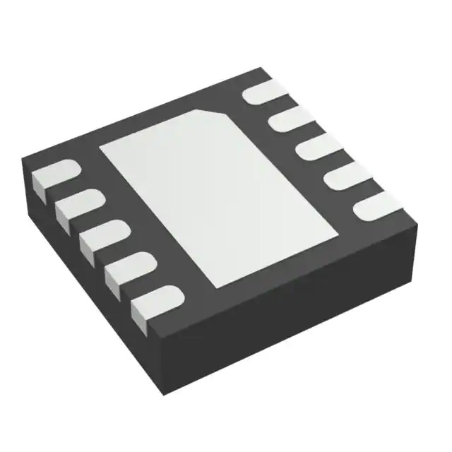
TPS74801DRCR (Hot offer) New TPS74801DRCR in stock
Product Attributes
| TYPE | DESCRIPTION |
SELECT |
| Category | Integrated Circuits (ICs) |
|
| Mfr | Texas Instruments |
|
| Series | - |
|
| Package | Tape & Reel (TR)
Cut Tape (CT) Digi-Reel® |
|
| Product Status | Active |
|
| Output Configuration | Positive |
|
| Output Type | Adjustable |
|
| Number of Regulators | 1 |
|
| Voltage - Input (Max) | 5.5V |
|
| Voltage - Output (Min/Fixed) | 0.8V |
|
| Voltage - Output (Max) | 3.6V |
|
| Voltage Dropout (Max) | 0.16V @ 1.5A |
|
| Current - Output | 1.5A |
|
| PSRR | 50dB ~ 30dB (1kHz ~ 300kHz) |
|
| Control Features | Enable, Power Good, Soft Start |
|
| Protection Features | Over Current, Over Temperature, Short Circuit, Under Voltage Lockout (UVLO) |
|
| Operating Temperature | -40°C ~ 125°C |
|
| Mounting Type | Surface Mount |
|
| Package / Case | 10-VFDFN Exposed Pad |
|
| Supplier Device Package | 10-VSON (3x3) |
|
| Base Product Number | TPS74801 |
|
| SPQ | 3000/pcs |
voltage regulator
A voltage regulator generates a fixed output voltage of a preset magnitude that remains constant regardless of changes to its input voltage or load conditions. There are two types of voltage regulators: linear and switching.
A linear regulator employs an active (BJT or MOSFET) pass device (series or shunt) controlled by a high gain differential amplifier. It compares the output voltage with a precise reference voltage and adjusts the pass device to maintain a constant output voltage.
A switching regulator converts the dc input voltage to a switched voltage applied to a power MOSFET or BJT switch. The filtered power switch output voltage is fed back to a circuit that controls the power switch on and off times so that the output voltage remains constant regardless of input voltage or load current changes.
Features for the TCAN1051V-Q1
- AEC Q100: Qualified for automotive applicationsMeets the ISO 11898-2:2016 and ISO 11898-5:2007 physical layer standards
- Temperature grade 1: -40°C to 125°C, TA
- HBM classification level: ±16 kV
- CDM classification level ±1500 V
- Functional Safety-Capable
- Documentation available to aid functional safety system design
- ’Turbo’ CAN:EMC performance: supports SAE J2962-2 and IEC 62228-3 (up to 500 kbps) without common mode choke
- All devices support classic CAN and 2 Mbps CAN FD (flexible data rate) and "G" options support 5 Mbps
- Short and symmetrical propagation delay times and fast loop times for enhanced timing margin
- Higher data rates in loaded CAN networks
- I/O Voltage range supports 3.3 V and 5 V MCUs
- Ideal passive behavior when unpowered
- Bus and logic terminals are high impedance (no load)
- Power up/down with glitch free operation on bus and RXD output
- Protection featuresReceiver common mode input voltage: ±30 V
- IEC ESD protection up to ±15 kV
- Bus Fault protection: ±58 V (non-H variants) and ±70 V (H variants)
- Undervoltage protection on VCC and VIO (V variants only) supply terminals
- Driver dominant time out (TXD DTO) - Data rates down to 10 kbps
- Thermal shutdown protection (TSD)
- Typical loop delay: 110 ns
- Junction temperatures from –55°C to 150°C
- Available in SOIC(8) package and leadless VSON(8) Package (3.0 mm x 3.0 mm) with improved automated optical inspection (AOI) capability
Description for the TCAN1051V-Q1
This CAN transceiver family meets the ISO11898-2 (2016) High Speed CAN (Controller Area Network) physical layer standard. All devices are designed for use in CAN FD networks up to 2 Mbps (megabits per second). Devices with part numbers that include the "G" suffix are designed for data rates up to 5 Mbps, and versions with the "V" have a secondary power supply input for I/O level shifting the input pin thresholds and RXD output level. This family of devices comes with silent mode which is also commonly referred to as listen-only mode. Additionally, all devices include many protection features to enhance device and network robustness.


