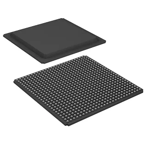
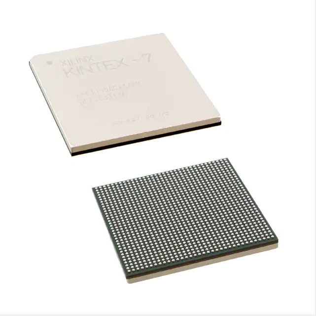
XC7Z030-2FFG676I – Integrated Circuits (ICs), Embedded, System On Chip (SoC)
Product Attributes
| TYPE | DESCRIPTION |
| Category | Integrated Circuits (ICs) |
| Mfr | AMD |
| Series | Zynq®-7000 |
| Package | Tray |
| Product Status | Active |
| Architecture | MCU, FPGA |
| Core Processor | Dual ARM® Cortex®-A9 MPCore™ with CoreSight™ |
| Flash Size | - |
| RAM Size | 256KB |
| Peripherals | DMA |
| Connectivity | CANbus, EBI/EMI, Ethernet, I²C, MMC/SD/SDIO, SPI, UART/USART, USB OTG |
| Speed | 800MHz |
| Primary Attributes | Kintex™-7 FPGA, 125K Logic Cells |
| Operating Temperature | -40°C ~ 100°C (TJ) |
| Package / Case | 676-BBGA, FCBGA |
| Supplier Device Package | 676-FCBGA (27x27) |
| Number of I/O | 130 |
| Base Product Number | XC7Z030 |
Documents & Media
| RESOURCE TYPE | LINK |
| Datasheets | Zynq-7000 All Programmable SoC Overview |
| Product Training Modules | Powering Series 7 Xilinx FPGAs with TI Power Management Solutions |
| Environmental Information | Xiliinx RoHS Cert |
| Featured Product | All Programmable Zynq®-7000 SoC |
| PCN Design/Specification | Mult Dev Material Chg 16/Dec/2019 |
| Errata | Zynq-7000 Errata |
Environmental & Export Classifications
| ATTRIBUTE | DESCRIPTION |
| RoHS Status | ROHS3 Compliant |
| Moisture Sensitivity Level (MSL) | 4 (72 Hours) |
| REACH Status | REACH Unaffected |
| ECCN | 3A991D |
| HTSUS | 8542.39.0001 |
Application Processor Unit (APU)
The key features of the APU include:
• Dual-core or single-core ARM Cortex-A9 MPCores. Features associated with each core include:
• 2.5 DMIPS/MHz
• Operating frequency range:
- Z-7007S/Z-7012S/Z-7014S (wire bond): Up to 667 MHz (-1); 766 MHz (-2)
- Z-7010/Z-7015/Z-7020 (wire bond): Up to 667 MHz (-1); 766 MHz (-2); 866 MHz (-3)
- Z-7030/Z-7035/Z-7045 (flip-chip): 667 MHz (-1); 800 MHz (-2); 1GHz (-3)
- Z-7100 (flip-chip): 667 MHz (-1); 800 MHz (-2)
• Ability to operate in single processor, symmetric dual processor, and asymmetric dual processor modes
• Single and double precision floating point: up to 2.0 MFLOPS/MHz each
• NEON media processing engine for SIMD support
• Thumb®-2 support for code compression
• Level 1 caches (separate instruction and data, 32 KB each)
- 4-way set-associative
- Non-blocking data cache with support for up to four outstanding read and write misses each
• Integrated memory management unit (MMU)
• TrustZone® for secure mode operation
• Accelerator coherency port (ACP) interface enabling coherent accesses from PL to CPU memory space
• Unified Level 2 cache (512 KB)
• 8-way set-associative
• TrustZone enabled for secure operation
• Dual-ported, on-chip RAM (256 KB)
• Accessible by CPU and programmable logic (PL)
• Designed for low latency access from the CPU
• 8-channel DMA
• Supports multiple transfer types: memory-to-memory, memory-to-peripheral, peripheral-to-memory, and scatter-gather
• 64-bit AXI interface, enabling high throughput DMA transfers
• 4 channels dedicated to PL
• TrustZone enabled for secure operation
• Dual register access interfaces enforce separation between secure and non-secure accesses
• Interrupts and Timers
• General interrupt controller (GIC)
• Three watch dog timers (WDT) (one per CPU and one system WDT)
• Two triple timers/counters (TTC)
• CoreSight debug and trace support for Cortex-A9
• Program trace macrocell (PTM) for instruction and trace
• Cross trigger interface (CTI) enabling hardware breakpoints and triggers


