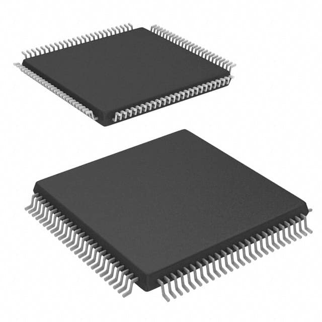
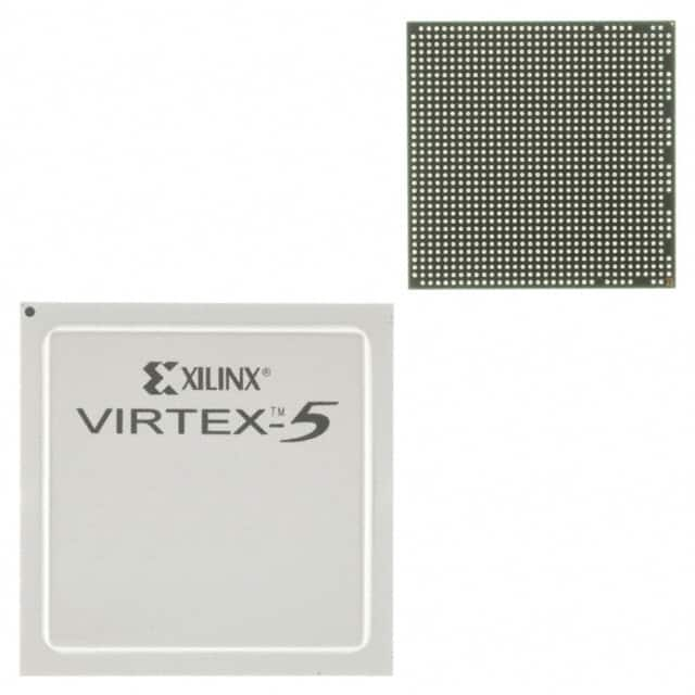
XCVU9P-2FLGA2104I – Integrated Circuits, Embedded, FPGAs (Field Programmable Gate Array)

Product Attributes
| TYPE | DESCRIPTION |
| Category | Integrated Circuits (ICs) |
| Mfr | AMD |
| Series | Virtex® UltraScale+™ |
| Package | Tray |
| Product Status | Active |
| DigiKey Programmable | Not Verified |
| Number of LABs/CLBs | 147780 |
| Number of Logic Elements/Cells | 2586150 |
| Total RAM Bits | 391168000 |
| Number of I/O | 416 |
| Voltage - Supply | 0.825V ~ 0.876V |
| Mounting Type | Surface Mount |
| Operating Temperature | -40°C ~ 100°C (TJ) |
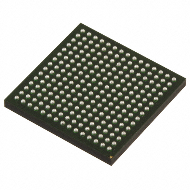
| Package / Case | 2104-BBGA, FCBGA |
| Supplier Device Package | 2104-FCBGA (47.5x47.5) |
| Base Product Number | XCVU9 |
Documents & Media
| RESOURCE TYPE | LINK |
| Datasheets | Virtex UltraScale+ FPGA Datasheet |
| Environmental Information | Xiliinx RoHS Cert |
| EDA Models | XCVU9P-2FLGA2104I by SnapEDA |
Environmental & Export Classifications
| ATTRIBUTE | DESCRIPTION |
| RoHS Status | ROHS3 Compliant |
| Moisture Sensitivity Level (MSL) | 4 (72 Hours) |
| ECCN | 3A001A7B |
| HTSUS | 8542.39.0001 |
FPGAs
Principle of operation:
FPGAs use a concept such as the Logic Cell Array (LCA), which internally consists of three parts: the Configurable Logic Block (CLB), the Input Output Block (IOB) and the Internal Interconnect. Field Programmable Gate Arrays (FPGAs) are programmable devices with a different architecture than traditional logic circuits and gate arrays such as PAL, GAL and CPLD devices. The logic of the FPGA is implemented by loading the internal static memory cells with programmed data, the values stored in the memory cells determine the logic function of the logic cells and the way in which the modules are connected to each other or to the I/O. The values stored in the memory cells determine the logical function of the logic cells and the way in which the modules are linked to each other or to the I/Os, and ultimately the functions that can be implemented in the FPGA, which allows unlimited programming.
Chip design:
Compared to other types of chip design, a higher threshold and a more rigorous basic design flow is usually required regarding FPGA chips. In particular, the design should be closely linked to the FPGA schematic, which allows for a larger scale of special chip design. By using Matlab and special design algorithms in C, it should be possible to achieve a smooth transformation in all directions and thus ensure that it is in line with current mainstream chip design thinking. If this is the case, then it is usually necessary to focus on the orderly integration of components and the corresponding design language to ensure a usable and readable chip design. The use of FPGAs enables board debugging, code simulation and other related design operations to ensure that the current code is written in a way and that the design solution meets the specific design requirements. In addition to this, the design algorithms should be prioritised in order to optimise the project design and the effectiveness of the chip operation. As a designer, the first step is to build a specific algorithm module to which the chip code is related. This is because pre-designed code helps to ensure the reliability of the algorithm and significantly optimises the overall chip design. With full board debugging and simulation testing, it should be possible to reduce the cycle time consumed in designing the entire chip at source and to optimise the overall structure of the existing hardware. This new product design model is often used, for example, when developing non-standard hardware interfaces.
The main challenge in FPGA design is to become familiar with the hardware system and its internal resources, to ensure that the design language enables the effective coordination of components and to improve the readability and utilisation of the program. This also places high demands on the designer, who needs to gain experience in multiple projects to meet the requirements.
The algorithm design needs to focus on reasonableness to ensure the final completion of the project, to propose a solution to the problem based on the actual situation of the project, and to improve the efficiency of the FPGA operation. After determining the algorithm should be reasonable to build the module, to facilitate the code design later. Pre-designed code can be used in code design to improve efficiency and reliability. Unlike ASICs, FPGAs have a shorter development cycle and can be combined with design requirements to change the structure of the hardware, which can help companies launch new products quickly and meet the needs of non-standard interface development when communication protocols are not mature.